Tomsk Polytechnic University scientists have made headway in studying the interactions between 2D materials at the nano-particle level, which will make it possible to develop advanced electronic components, including flexible displays for devices, solar batteries and other innovative technologies, the University’s press service told Sputnik.
Tomsk Polytechnic University scientists and their German colleagues are the first to show how 2D advanced electronic materials-components interact at the nano-particle level. Their survey results are published in Nano-Letters.
This new technology will make it possible to calculate strains during interaction between materials and even to identify nano-level defects.
This data can be used to upgrade tiny modern electronic components that are used in developing flexible displays for electronic devices, flexible optical and computer circuits, solar batteries and other innovative technologies, said Professor Raul Rodriguez from the University’s Faculty of Laser and Lighting Equipment.
“We need various classes of 2D materials, including semiconductors, to create a full line of essential electronic devices. We worked with molybdenum disulfide, one the most popular 2D semiconductors. We studied the nano-level strains in this material, as well as expansion or contraction processes in various structures,” he told Sputnik.
To accomplish this, the scientists used gold nano-particles or nano-triangles. They placed two mono-layers of molybdenum disulfide on these nano-triangles. Due to the bulging form of these nano-triangles, the layer became deformed and this caused 1.4 percent local strains.
“This is more than we had initially expected. To be honest, we weren’t trying to obtain the highest possible strain. It may be interesting, but it is possible to obtain such impressive deformations by placing thin molybdenum disulfide layers on a metal surface. While creating nano-devices, it is very important to understand what happens when the semiconductor (molybdenum disulfide) and the conductor (gold) contact each other,” Professor Rodriguez said.
“We shouldn’t discount the interaction between a thin film and substrates in nano-devices,” he noted.
“When these materials are studied, all of their electronic, zonal and optical properties are analyzed on a flat substrate. But the presence of metals that can act as electrodes inevitably changes the material’s properties,” the scientist added.
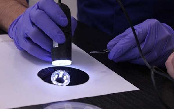
The experiment involved the unique Tip-Enhanced Raman Spectroscopy (TERS) technology combining methods of optical spectroscopy and atomic-force microscopy. A gold nano-antenna inside an atomic-force microscope is the main TERS element. The foundation has a diameter of several microns, and the tip’s size is several nano-meters.
“Imagine a group of nano-particles illuminated by a laser beam. The laser spot measures about two microns, and the average diameter of one nano-particle is 40 nano-meters. The laser beam allows us to categorize nano-particles in the immediate vicinity we’re studying. As the laser spot’s diameter exceeds that of nano-particles, we will obtain an average signal and will be unable to distinguish between them. But, it is possible to obtain the signal from a nano-particle located on the nano-antenna’s tip,” Professor Rodriguez explained.
Today, Germany manufactures these nano-antennas, but scientists have already announced plans to re-locate the production to Tomsk Polytechnic University soon.
Sourse: sputniknews.com