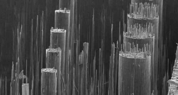
A unique silicon-based nanostructured composite created by scientists from the National University of Science and Technology “MISiS” (NUST MISIS) in cooperation with their colleagues from the Russian Academy of Sciences will accelerate the development of “micropower plants” technology embedded directly in printed circuit boards of electronics.
The results of the study were published in the Microporous and Mesoporous Materials Journal.
According to scientists, porous silicon structures are increasingly being used in microelectronics and biomedicine. Their key property is the smooth distribution of pores of different sizes throughout the material, from nanoporous layers on the surface to the macroporous frame.
In medicine, porous silicon membranes play the role of filters, for example for haemodialysis. In portable electronics, they are used as electrodes for micro fuel cells – a prospective hydrogen energy source that can be integrated into printed circuit boards.
However, the nanoporous silicon gradually degrades in contact with working fluids such as water or weakly alkaline solutions. Scientists at NUST MISIS in collaboration with the Institute of Microelectronics Technology and High-Purity Materials of the Russian Academy of Sciences (IPTM RAS) have developed a unique technique to radically improve the properties of porous silicon membranes through the application of graphene coating.
The new technology reduces the surface electrical resistance of silicon structures by several hundred times and significantly increases their resistance to weak alkaline solutions. In addition, the formation of additional topography inside the pores increases the useful surface area of the material more than three times. The scientists explained that this dramatically increases the performance of the micro fuel cell and improves the longevity of the expensive catalysts used in it.
An original CVD synthesis process from alcohol vapour was used to create the coating, the authors of the technology said. They claimed that the proposed method is distinguished by the use of a “sharp pressure drop” (SPD) mode in the reactor working zone, which ensures the deposition of graphene even in layers with closed nanopores.
The new technology is protected by RF Patent No. 2731278, issued on 1 September 2020. The research results were presented at the 24th Moscow International Inventions and Innovative Technologies Salon “Archimedes” in 2021. In the future, the research team intends to adopt the technology for industrial applications.
Sourse: sputniknews.com


